
July 1, 2026
The Upstream Chokepoint: How a Single Compound Is Gating the AI Hardware Revolution
The semiconductor industry has spent decades worrying about finished chip shortages, fab capacity, and lithography tool bottlenecks. What it did not fully anticipate was a scenario where the constraint sits one level further upstream, at the compound semiconductor substrate layer, in a material most people have never heard of. Indium phosphide has quietly become one of the most consequential materials in modern AI infrastructure, and China indium phosphide export controls introduced in February 2025 are now reverberating across data centre construction timelines worldwide.
Understanding why this matters requires stepping back from the headlines and examining the physical architecture of modern AI computing, where the chokepoint actually sits, and why the usual market remedies, such as finding new suppliers or substituting materials, are far more constrained than most observers initially assumed.
When big ASX news breaks, our subscribers know first
Why Photonics Replaced Copper and Why InP Is Central to That Shift
For most of computing history, servers and networking equipment communicated using electrical signals carried through copper interconnects. As AI workloads have grown in intensity, particularly the massive parallel processing required for training large language models and running inference at hyperscale, copper has become a performance bottleneck. Electrical signals degrade over distance, generate significant heat, and consume disproportionate power at the bandwidth levels modern AI clusters demand.
Photonics solves these problems by transmitting data as light rather than electrical current, using fiber-optic pathways that carry information at speeds and distances copper cannot match. Optical transceivers, the devices that convert electrical signals to light and back again, are now critical components inside every serious AI data centre. Furthermore, the substrate material that makes high-speed optical transceivers and laser components physically possible at commercial scale is indium phosphide.
The Physical Properties That Make InP Genuinely Irreplaceable
InP is not irreplaceable simply because alternatives have not been explored. It possesses a direct bandgap structure that makes it highly efficient at emitting and detecting light at the wavelengths used in fibre-optic communications, specifically around 1,300 to 1,550 nanometres. This property allows InP-based lasers and photodetectors to operate at speeds exceeding 100 gigabits per second per channel, with energy efficiency that silicon photonics and gallium arsenide alternatives cannot currently match for this specific application.
Silicon photonics, which uses standard silicon wafer fabrication to build optical components, is a genuine competitor in some transceiver segments, but it still requires InP-based laser sources for light generation. Gallium arsenide offers comparable electron mobility but operates at the wrong wavelength range for long-haul and medium-reach data centre interconnects. The result is a material that occupies a specific performance niche with no commercially available drop-in replacement.
Konrad Wang, a research analyst at SemiAnalysis, has described InP as one of several supply chain bottlenecks collectively gating AI data centre buildouts, a characterisation that reflects growing industry consensus about the compound's structural importance to the photonics layer of AI infrastructure.
China Indium Phosphide Export Controls: The Architecture of the Restriction
China indium phosphide export controls introduced in February 2025 do not ban shipments outright. Instead, they require exporters to obtain government-issued licences before shipping InP substrates, wafers, crystals, and related compounds to overseas customers. This licensing mechanism is subtler than an outright embargo and, in some ways, more effective as a trade instrument.
By creating administrative friction rather than a hard prohibition, Beijing can modulate the flow of material, slow qualification timelines, and generate procurement anxiety, all without triggering the formal trade dispute mechanisms that a complete ban would invite. The design is consistent with a broader strategic pattern that Paul Triolo, Partner at the Albright Stonebridge Group, has characterised as a more granular materials chokepoint toolkit, one that targets upstream compounds and substrates to condition whether the downstream photonics ecosystem can scale fast enough to meet hyperscaler demand. According to recent analysis of China's export restriction approach, these controls are already disrupting optical communications materials supply chains globally.
How InP Controls Fit Within China's Broader Export Playbook
The InP restrictions did not emerge in isolation. China had already deployed export controls on rare earth elements, gallium, germanium, and graphite in preceding years, with each round targeting materials where Chinese production is concentrated and where downstream industries in Western nations have limited alternative sources. The sequencing reveals a deliberate escalation from bulk commodities toward higher-value processed compounds, where switching costs and qualification timelines are longest.
China's export controls strategy follows a consistent logic across multiple materials. China accounts for approximately 70% of global indium output as of 2024, according to the US Geological Survey. For InP substrates specifically, the concentration is even more acute because substrate manufacturing requires sophisticated crystal growth expertise that took years to develop and cannot be replicated quickly elsewhere.
The Global InP Substrate Market: Concentration and Fragility
The structure of the global InP substrate market is unusually concentrated even by semiconductor industry standards. Two producers, AXT Inc. and Sumitomo Electric Industries of Japan, together account for approximately 80% of global InP substrate manufacturing capacity.
| Supplier | Estimated Global InP Substrate Share | Key Notes |
|---|---|---|
| AXT Inc. | ~40–45% | Manufactures primarily in China; first export permits received June 2024 |
| Sumitomo Electric Industries | ~35–40% | Japanese producer; significant internal consumption limits open-market supply |
| JX Advanced Metals | ~10% | Smaller-scale producer; limited capacity expansion data |
| Other / Emerging | ~10–15% | Includes Chinese domestic producers with export restrictions |
The Internal Consumption Problem
What makes Sumitomo's position particularly important to understand is that its production figures overstate available open-market supply. A person familiar with China's photonic chip industry has noted that Sumitomo consumes a substantial portion of its substrate output internally for its own photonics manufacturing operations. This internal consumption dynamic means the global market available to third-party buyers is materially smaller than headline production numbers suggest, consequently compounding the tightness created by China's export licensing regime.
AXT presents a different structural vulnerability. The company manufactures the majority of its InP substrates inside China, meaning its ability to supply customers depends directly on the pace at which Chinese authorities issue export permits. AXT's Chinese subsidiary did not receive its first export permits until June 2024, and the company has subsequently carried a significant order backlog, reflecting the administrative lag between demand and approved export volumes.
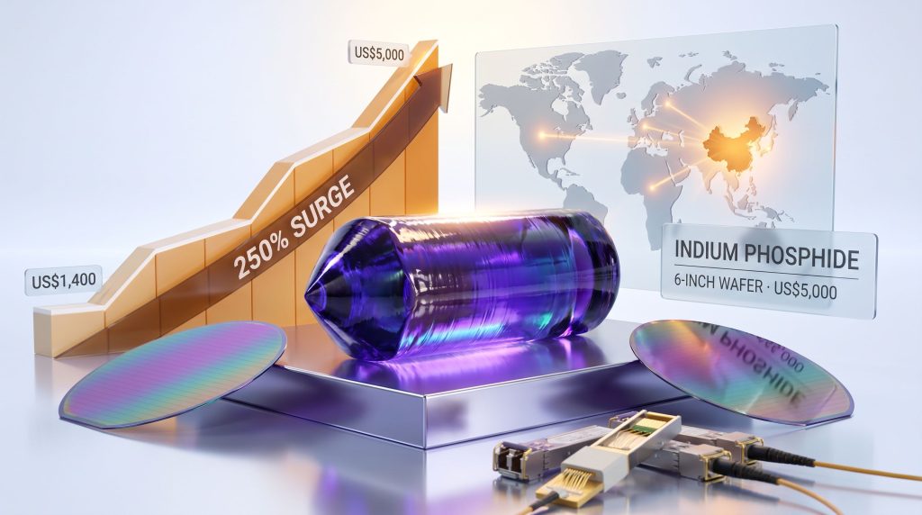
The Price Signal: What a 250% Wafer Price Surge Tells Investors
Price movements in niche industrial materials often tell a more complete story than supply chain commentary alone. Since the China indium phosphide export controls took effect in February 2025, the price of a 6-inch InP wafer has risen from approximately US$1,400 to US$5,000, a 250% increase that reflects both genuine physical tightness and the procurement behaviour of manufacturers buying ahead of anticipated shortages.
This type of dual-driver price surge, genuine scarcity combined with precautionary stockpiling, tends to overshoot equilibrium in the short term before settling at a structurally higher level once the market adjusts. For investors tracking photonics supply chains, the critical minerals demand surge feeding into InP is central to understanding whether wafer prices stabilise near current levels or retreat as alternative supply comes online. Given the capacity timelines discussed below, stabilisation at elevated levels appears more likely than a near-term correction.
Company-Level Exposure Across the Photonics Supply Chain
The export controls have created differentiated exposure across companies depending on where they sit in the value chain and how much of their substrate supply passes through Chinese licensing procedures.
| Company | Primary Exposure | Mitigation Status |
|---|---|---|
| Coherent | Direct InP substrate dependency; manufacturing in US | Doubling Texas wafer capacity; CEO joined US-China diplomatic delegation |
| Lumentum | Demand exceeds supply through 2028 | Quadrupled output; capacity ceiling remains a constraint |
| AXT | Manufactures substrates in China; export permit delays | First permits received June 2024; backlog persists |
| LandMark Optoelectronics | Substrate supply disruptions via AXT delays | Signed long-term supply agreement with Sumitomo (April 2025) |
| VPEC | Indirect exposure via substrate supply chain | Mitigation strategy not publicly disclosed |
Coherent and the Diplomatic Dimension
The urgency of the InP shortage became visible at the geopolitical level when Coherent's CEO joined a US business delegation accompanying President Donald Trump to China following a May 2025 earnings call in which the company flagged InP supply constraints. The issue was also raised in Seoul during preliminary trade negotiations between US and Chinese officials ahead of the Trump-Xi summit. The elevation of a substrate material to summit-level trade agenda items signals how deeply the photonics supply chain disruption has penetrated policy circles.
Coherent is pursuing domestic capacity expansion, doubling InP wafer production at its Texas facility in 2025 and planning to more than double capacity again by the end of 2027. Nvidia has committed US$2 billion investments each into Coherent and Lumentum, a capital signal reflecting how seriously hyperscalers view photonics supply security. Marvell Technology's acquisition of semiconductor startup Celestial AI further illustrates the industry-wide bet that photonic interconnects will define next-generation AI hardware architecture.
Lumentum: Sold Out Through 2028
Lumentum's situation illustrates the demand-supply mismatch in stark terms. Despite quadrupling production output, the company remains sold out through 2028. This is not a demand forecasting anomaly — it reflects the fundamental reality that InP substrate availability has become the ceiling on how fast photonics manufacturers can grow, regardless of their own fabrication investments.
The next major ASX story will hit our subscribers first
Can Western Capacity Expansion Solve the Supply Problem?
The honest answer is: not quickly. Building a new InP substrate manufacturing facility from greenfield to commercial production is a multi-year undertaking that involves far more than constructing a building and installing equipment. Indeed, the processing bottlenecks facing compound semiconductor materials share structural similarities with those seen across other critical mineral supply chains.
Step-by-Step: How a New InP Wafer Facility Reaches Commercial Production
- Site selection and regulatory approval — typically 6 to 12 months depending on jurisdiction
- Equipment procurement and installation — 12 to 18 months for specialised crystal growth systems including Czochralski or liquid encapsulated Czochralski (LEC) pullers
- Initial crystal growth trials — 6 to 12 months to achieve target material specifications including carrier concentration, dislocation density, and wafer uniformity
- Customer qualification testing — 12 to 24 months for tier-one photonics manufacturers who must validate that new substrate sources do not degrade device performance
- Volume ramp to commercial scale — additional 6 to 12 months post-qualification
- Total timeline to meaningful supply contribution — 2.5 to 4 years from a greenfield start
The qualification cycle is particularly important and frequently underappreciated. Photonics manufacturers cannot simply switch substrate suppliers the way commodity purchasers switch vendors. The crystallographic properties of the wafer, including dislocation density, surface roughness, dopant uniformity, and stoichiometric precision, directly affect the performance characteristics of the finished laser or transceiver. Each new substrate source must be exhaustively tested and validated, a process that typically takes one to two years even when the new material is technically equivalent.
This qualification barrier means that even if new InP substrate capacity is available by 2026 or 2027, it cannot flow into the supply chain as usable product until qualification is complete, pushing meaningful alternative supply contribution toward 2027 to 2028 at the earliest.
Chinese Domestic Producers: Filling the Export Gap at Home
While Chinese InP manufacturers face restrictions on overseas shipments, the controls have created an opening for domestic capacity expansion serving China's own photonics industry. Three producers are notable in this context.
- Yunnan Germanium announced a 189 million yuan (approximately US$28 million) investment in April 2025 to expand InP wafer capacity to 450,000 wafers annually, following a 74% surge in shipments in 2025. The shipment surge primarily reflects domestic Chinese demand rather than export growth, suggesting that China's own AI infrastructure buildout is absorbing expanded production capacity.
- Guangdong Xiandao, through its subsidiary Guangdong Xianrui, launched a project targeting 40 tonnes of InP crystals per year, a meaningful volume addition focused on the upstream crystal growth stage.
- Zhuhai Dingtai Xinyuan represents a third domestic producer expanding into the space as domestic demand justifies additional capacity.
A source at a major Chinese InP manufacturer has indicated that overseas shipments from these producers are likely to remain structurally limited, both because domestic demand is absorbing output and because the lengthy qualification cycles required by overseas customers create a practical barrier to rapid market entry even when export approvals are granted.
InP Constraints and the AI Data Centre Buildout Timeline
The interaction between InP supply constraints and AI infrastructure expansion creates a compounding problem. Optical transceivers are not optional components in modern AI clusters. As hyperscalers build out rack-scale AI systems requiring thousands of high-bandwidth interconnects, transceiver availability becomes a deployment gating factor. A shortage at the substrate level propagates upward through transceiver availability to data centre commissioning timelines.
Hypothetical Scenario: InP Supply Remains Constrained Through 2027
- Hyperscalers face optical transceiver shortages that delay rack-scale AI cluster deployments, particularly for high-bandwidth spine-leaf network architectures
- InP wafer prices stabilise in the US$4,000 to US$6,000 range as limited alternative supply prevents a return to pre-restriction price levels
- Western governments accelerate critical mineral designation frameworks for indium and InP compounds, enabling co-investment vehicles for domestic substrate manufacturing
- New substrate manufacturing investments in the US, Japan, and allied nations begin construction, with commercial output targeted for 2027 to 2028
- Chinese domestic photonics producers gain a 12 to 24 month technological advantage in InP-based chip development, benefiting from uninterrupted substrate access while overseas competitors manage supply disruptions
Disclaimer: The scenario above represents a hypothetical analytical framework based on current supply chain dynamics and publicly available information. It does not constitute investment advice or a forecast of future events. Actual outcomes will depend on diplomatic developments, regulatory decisions, and market conditions that cannot be predicted with certainty.
Mineral-Producing Nations and the Concession Stability Imperative
The InP chokepoint has elevated a question that mineral-producing nations outside China are increasingly being asked to answer: how secure are your concession regimes for investors seeking to develop indium-bearing assets? This concern connects directly to the broader geopolitical metals landscape, where supply chain sovereignty has become a defining policy objective.
Indium is not typically mined as a primary product. It occurs predominantly as a trace element in sphalerite, the primary zinc ore mineral, and is recovered as a by-product of zinc smelting. Nations with significant zinc mining operations, including Canada, South Korea, Belgium, and several Latin American countries, therefore have theoretical indium production potential that depends on smelting capacity, recovery technology, and the economic incentive structure created by indium prices.
Mexico presents an instructive case study in the intersection of regulatory enforcement and critical mineral investment attractiveness. In February 2025, Mexican federal authorities reported that 1,126 mining concessions covering 889,512 hectares across six states had been cancelled through administrative procedures, with 713 concessions located within Natural Protected Areas.
The primary grounds for cancellation were non-payment of mining duties for two consecutive fiscal years and failure to submit mandatory statistical and technical reports. Under Article 42 of Mexico's Mining Law, these represent formal legal grounds for concession termination. Santiago Suárez Sevilla, Partner at Servicios Legales Mineros, has noted through analysis published by Mexico Business News that affected concessionaires retain multiple remedies, including administrative review proceedings, recourse before the Federal Administrative Justice Court, and amparo actions under constitutional law.
For investors evaluating indium-related critical mineral assets globally, the lesson is not that Mexico is uniquely risky, but rather that compliance with concession reporting and payment obligations has become a material investment consideration as governments tighten enforcement frameworks. In an environment where supply chain diversification away from Chinese critical mineral dominance is a strategic priority for multiple governments, jurisdictions that combine mineral prospectivity with clear, enforceable, and consistently administered concession regimes hold a meaningful competitive advantage in attracting long-term capital.
Frequently Asked Questions: China Indium Phosphide Export Controls
What Are China's Indium Phosphide Export Controls?
China introduced licensing requirements for indium phosphide exports beginning in February 2025. The regime requires manufacturers and traders to obtain government-issued permits before shipping InP substrates, wafers, crystals, and related compounds to international customers. The controls form part of a broader expansion of China's critical materials export management framework, extending a playbook previously applied to rare earths, gallium, and germanium. Detailed reporting on China's indium phosphide controls and AI supply chains underscores the far-reaching consequences for the semiconductor and photonics industries.
How Much Has the InP Wafer Price Increased?
Since the controls took effect in February 2025, the price of a 6-inch InP wafer has risen approximately 250%, reaching US$5,000 per unit from an estimated US$1,400 prior to the licensing regime. This increase reflects both genuine supply tightness from permit delays and precautionary procurement behaviour by photonics manufacturers seeking to build buffer inventory.
What Is the Difference Between Indium Metal and Indium Phosphide Substrates?
Indium metal is the elemental raw material recovered primarily as a by-product of zinc smelting. Indium phosphide is a compound semiconductor created by combining purified indium with phosphorus under controlled high-temperature and high-pressure conditions, a technically demanding process requiring specialised crystal growth equipment and deep metallurgical expertise. China's export controls target InP compounds and substrates rather than raw indium metal, focusing the restriction on the value-added processing stage where Chinese industrial capacity is most concentrated and most difficult to replicate overseas.
Which Countries Produce Indium Outside of China?
Meaningful indium production occurs in South Korea, Canada, Japan, and Belgium, primarily as a zinc smelting by-product. These sources collectively account for approximately 30% of global output. However, none currently manufactures InP substrates at the scale required to offset Chinese supply constraints, and the gap between raw indium availability and finished substrate production involves substantial additional processing capability that does not currently exist at sufficient scale outside China and Japan.
How Long Will It Take to Build Alternative InP Supply Capacity?
Based on industry construction and qualification timelines, new InP substrate manufacturing facilities require approximately two to three years from construction commencement to reach commercial-scale production, followed by an additional 12 to 24 months for customer qualification at major photonics manufacturers. Meaningful alternative supply is therefore unlikely to reach the market before 2027 to 2028 at the earliest, even assuming construction begins promptly and proceeds without regulatory or technical delays.
Structural Implications: What the InP Chokepoint Reveals About Supply Chain Architecture
The China indium phosphide export controls reveal a vulnerability in the global semiconductor supply chain architecture that extends well beyond InP itself. The pattern — in which a single jurisdiction controls a dominant share of upstream compound processing, creating a chokepoint that downstream manufacturers cannot quickly route around — is not unique to InP. It applies across multiple compound semiconductor materials where China's processing capacity has grown to dominate global supply over the past two decades. Consequently, the role of critical minerals for semiconductors has moved to the centre of allied nations' industrial policy agendas.
For policymakers, the lesson is that supply chain resilience requires attention at the compound and substrate level, not just at the finished chip or device level. For investors, the InP situation illustrates the growing strategic premium attached to companies and jurisdictions that can credibly reduce dependence on single-source upstream materials. And for the AI industry itself, the InP shortage is a reminder that the pace of the AI infrastructure buildout is ultimately constrained not by compute design or software capability, but by the physical availability of the materials that make photonic hardware possible.
The two to four year timeline to meaningful alternative substrate supply means that photonics companies, hyperscalers, and their investors are navigating a period of structural tightness that will not resolve quickly regardless of capital commitments or diplomatic activity. Managing within that constraint, while building the longer-term diversification that makes future chokepoints less damaging, is now one of the defining strategic challenges facing the global AI hardware ecosystem.
Want to Stay Ahead of the Next Critical Mineral Disruption Before the Market Moves?
Discovery Alert's proprietary Discovery IQ model scans ASX announcements in real time, instantly identifying significant mineral discoveries across critical commodities — including those underpinning the photonics and semiconductor supply chains reshaping AI infrastructure — and delivering actionable alerts to subscribers before the broader market catches on. Explore historic examples of major mineral discoveries and their market returns, then start your 14-day free trial at Discovery Alert to position yourself ahead of the next critical minerals opportunity.