
June 13, 2026
The Invisible Material at the Heart of Every Semiconductor
Few materials science decisions carry more downstream consequence than the choice of what contains the melt during crystal growth. Long before a silicon wafer reaches a chip fabrication plant, before sapphire glass is cut into a smartphone screen, and before an optical crystal is shaped into a medical imaging component, every atom in that crystal passed through a crucible operating at temperatures most metals cannot survive. Understanding platinum in crystal growth for electronics and optics reveals a supply chain dependency with implications extending well beyond the laboratory.
The process that makes modern electronics possible is largely invisible to the people who use its outputs. Yet industrially-grown single crystals sit at the upstream origin of the global semiconductor supply chain, the LED lighting industry, precision optics, and advanced sensing technologies. Furthermore, understanding which material makes that process possible, and why no cheaper substitute has displaced it, reveals just how interconnected these dependencies truly are.
When big ASX news breaks, our subscribers know first
What Industrial Crystal Growth Actually Involves
Crystal growth, in an industrial context, is the controlled process of arranging atoms or molecules into highly ordered solid structures, according to the World Platinum Investment Council. That definition sounds deceptively simple. In practice, it requires engineering temperature environments within fractions of a degree, selecting container materials that will not react with aggressive molten feedstocks, and sustaining these conditions across production cycles that may last days.
What distinguishes a grown crystal from a natural mineral or an amorphous solid is structural perfection. When atoms self-assemble into a repeating lattice with minimal defects and dislocations, the resulting material exhibits predictable, consistent electrical, optical, and mechanical properties. That predictability is exactly what semiconductor manufacturers, optics producers, and sensor designers require.
A crystal with irregular grain boundaries, incorporated impurities, or lattice defects behaves unpredictably. In a semiconductor wafer, unpredictability translates directly to yield loss, device failure, and commercial rejection. The entire value proposition of industrial crystal growth rests on achieving and maintaining structural and chemical perfection at scale.
Where Grown Crystals Appear Across Technology Sectors
The range of end-use applications for industrially-grown crystals is broader than most people outside the materials science community appreciate.
| End-Use Application | Crystal Type | Industry Sector |
|---|---|---|
| Semiconductor wafers | Monocrystalline silicon | Electronics / Computing |
| Scratch-resistant screens | Sapphire | Consumer electronics |
| LED lighting systems | Oxide crystals | Lighting / Display |
| Medical imaging equipment | Scintillator crystals | Healthcare |
| Advanced sensors | Optical crystals | Defence / Industrial |
| Solar photovoltaic cells | Monocrystalline silicon | Renewable energy |
| Frequency control components | Quartz / synthetic crystals | Telecommunications |
The World Platinum Investment Council notes that industrially-grown crystals are found in smartphones, computers, LED lighting systems, medical imaging equipment, and advanced sensors, with each application demanding a different crystal type and growth method.
Why Contamination Is the Defining Challenge
Purity is not merely a quality preference in crystal production. It is a functional threshold. Even trace metallic contamination at the parts-per-billion level can alter the electrical characteristics of semiconductor-grade silicon to the point where wafers become commercially unusable. Foreign atoms incorporated into a crystal lattice during growth disrupt the uniform atomic ordering that gives the material its functional properties.
This is why crucible material selection is among the most consequential decisions in crystal manufacturing. Whatever container holds the molten feedstock will be in sustained contact with a chemically aggressive liquid at extreme temperatures. Any reactivity, any dissolution of crucible material into the melt, transfers directly into the growing crystal.
How the Two Dominant Growth Methods Work
Two techniques account for the majority of commercial single crystal production globally: the Czochralski method and the Kyropoulos method. Both involve heating raw materials to exceptionally high temperatures, and both rely on the controlled interaction between a seed crystal and a molten feedstock. The critical difference lies in the direction and mechanism of crystal growth.
The Czochralski Process: Pulling Crystals Upward
The Czochralski method operates through a sequence of precisely controlled steps:
-
Raw feedstock material is loaded into a crucible and heated until fully molten.
-
A small seed crystal with a known atomic orientation is lowered until it contacts the molten surface.
-
The seed is slowly rotated and withdrawn upward at a controlled rate, pulling a cylindrical ingot from the melt.
-
Careful management of temperature gradients and pull speed allows the solidification front to advance with consistent atomic alignment.
The primary output of this process is large-diameter silicon ingots, which are subsequently sliced into wafers for semiconductor fabrication. The Czochralski method is also used to produce synthetic gemstones such as yttrium aluminium garnet (YAG) and alexandrite, as well as optical crystals for specialised applications. The technique has remained the dominant method for silicon production since its development in the early twentieth century, a testament to its reliability and scalability.
The Kyropoulos Process: Growing Crystals Downward
The Kyropoulos method follows a fundamentally different growth logic:
-
A seed crystal is introduced into the molten feedstock from above.
-
Rather than being extracted upward, the crystal grows downward into the melt as thermal conditions change.
-
Temperature is gradually and precisely reduced, driving crystallisation without mechanical extraction.
-
Once solidification is complete, the resulting boule is harvested from the crucible.
The primary output of Kyropoulos growth is large sapphire boules, used for optical windows, scratch-resistant display surfaces, and industrial components requiring high hardness combined with optical clarity. For a broader overview of crystal growth techniques applicable to optical applications, there is a growing body of technical literature exploring how these methods compare across different material systems.
A Side-by-Side Comparison
| Feature | Czochralski Method | Kyropoulos Method |
|---|---|---|
| Crystal growth direction | Upward (pulled from melt) | Downward (grown into melt) |
| Primary crystal output | Silicon ingots | Sapphire boules |
| Temperature management | Continuous high-temperature melt | Gradual temperature reduction |
| Key end-use | Semiconductors, solar cells | Optical windows, display screens |
| Crucible stress profile | High mechanical and thermal stress | Sustained thermal stress |
The downward-growth mechanism in the Kyropoulos method produces structurally distinct crystal characteristics compared to the Czochralski pull technique, reflecting the different thermal gradients, convection dynamics, and solidification kinetics involved in each approach. Crucible stress profiles also differ: Czochralski systems subject equipment to combined mechanical and thermal stress from the pulling operation, while Kyropoulos equipment must sustain prolonged thermal exposure without the added mechanical loading.
Why Platinum Is the Preferred Crucible Material
The Environment Inside a Crystal Growth Furnace
Operating a crystal growth furnace is an exercise in materials engineering at extremes. Silicon crystal growth requires temperatures exceeding 1,400°C. Oxide crystals used in sensors and optics require growth environments exceeding 2,000°C. At these temperatures, the molten feedstocks are not passive liquids. The World Platinum Investment Council describes them as highly corrosive and reactive, capable of degrading conventional container materials and introducing contamination into the growing crystal.
Most metals melt well below these temperatures. Many that survive thermally will react chemically with specific molten feedstocks. Others may remain physically intact while slowly dissolving trace quantities of their own material into the melt, a contamination pathway that is often difficult to detect and extremely difficult to reverse once it reaches the growing crystal.
Platinum's Physical and Chemical Advantages
Platinum occupies a rare position among industrially available materials. Its combination of properties addresses almost every challenge the crystal growth environment presents:
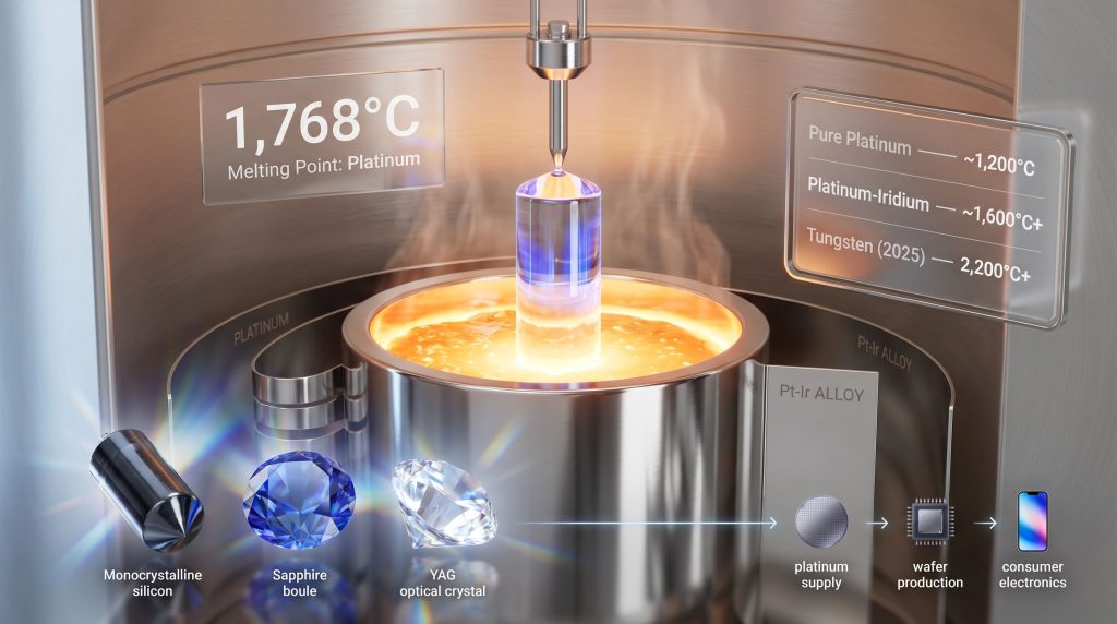
- Melting point of 1,768°C, enabling stable operation across most commercial crystal growth temperature ranges
- Chemical inertness against the majority of molten crystal feedstocks, preventing contamination of the growing crystal
- Mechanical strength retention at sustained extreme temperatures, maintaining structural integrity through extended production cycles
- Non-contaminating characteristics, meaning platinum does not leach impurities into the melt even under prolonged thermal stress
- Engineering versatility, allowing fabrication into precision crucibles, wires, ribbons, sheets, and baffles for various components within the growth system
The World Platinum Investment Council is explicit on the contamination point: platinum does not contaminate the growing crystal, helping achieve the ultrahigh purity that end applications demand. This is not simply a performance advantage. At the contamination thresholds that semiconductor and precision optical applications require, it is a functional prerequisite. The role of platinum in crystal growth for electronics and optics is, consequently, one of the most technically specific and commercially essential applications for the metal globally.
Beyond the Crucible: Platinum Throughout the Growth System
Crucibles represent only one part of the platinum demand within a crystal growth system. The World Platinum Investment Council identifies several additional components where platinum's properties are equally essential:
- Hydraulic stylus components: Platinum-tipped instruments that manipulate seed crystal positioning with micron-level precision during the initiation phase of crystal growth
- Radiation baffles: Engineered platinum shields that manage and direct heat radiation within the growth chamber, maintaining the thermal gradients required for consistent crystallisation
- Semi-finished product forms used in manufacturing these components include platinum wire, platinum ribbon, and platinum sheet, each engineered to specific dimensional and compositional tolerances
"The non-contaminating property of platinum is not merely a performance advantage. It is a fundamental requirement. Even parts-per-billion levels of metallic contamination can render semiconductor-grade crystals commercially unusable."
How Platinum Alloys Extend the Performance Envelope
The Limits of Pure Platinum
Pure platinum performs reliably as a crucible material up to approximately 1,200°C under continuous use in chemically aggressive conditions. Beyond this threshold, softening and mechanical deformation under sustained load become operational risks. For crystal growth processes that operate at the upper boundary of platinum's thermal range, or that subject crucibles to extended cycles, pure platinum may not provide the mechanical durability required for economical production.
Platinum-Iridium and Platinum-Rhodium Alloys
Additions of other platinum group metals address these limitations by modifying the alloy's mechanical and chemical characteristics:
| Alloy System | Key Benefit | Primary Application Risk |
|---|---|---|
| Pure Platinum | Zero contamination risk | Mechanical softening above ~1,200°C |
| Platinum-Iridium | Superior hardness and high-temperature strength | Potential iridium incorporation in specific melt chemistries |
| Platinum-Rhodium | Enhanced oxidation resistance and structural stability | Rhodium reactivity with certain feedstock materials |
Iridium additions significantly increase crucible hardness and extend service life in demanding applications. Rhodium enhances oxidation resistance and maintains structural stability at elevated temperatures. The World Platinum Investment Council confirms that iridium and rhodium can be alloyed with platinum to further enhance strength and crucible lifetime under extreme temperatures.
However, alloy selection requires careful application-specific analysis. Research has demonstrated that crucible material directly affects crystal composition in some systems. Iridium crucibles, for instance, produce measurably different crystal characteristics than platinum crucibles when growing iridate compounds, because iridium can be incorporated into the crystal lattice under certain thermodynamic conditions. This underscores why material selection in crystal growth is a precision engineering decision, not simply a procurement choice.
Alloy composition is calibrated across three competing requirements: thermal performance, chemical compatibility with the specific melt chemistry in use, and the acceptable risk threshold for alloying element incorporation into the product crystal.
Emerging Challenges at the High-Temperature Frontier
Where Platinum and Its Alloys Reach Their Limits
Growing demand for certain oxide single crystals requires growth temperatures above 2,000°C, and some novel materials being researched for next-generation electronics and photonics applications require temperatures above 2,200°C. At these levels, even platinum-iridium alloys approach the boundaries of practical application. Consequently, the industry is actively exploring alternative solutions for these extreme temperature environments.
Iridium alone, with a melting point of approximately 2,446°C, is substantially more brittle than platinum, limiting its fabricability into complex crucible geometries. It is also significantly more costly and presents contamination risks in specific melt chemistries, requiring careful application-specific evaluation.
Tungsten Crucible Development: A 2025 Breakthrough
In 2025, researchers at Tohoku University announced a development in tungsten crucible technology capable of sustained operation above 2,200°C. The advance addressed contamination and unwanted chemical reactions that had previously made tungsten impractical for precision crystal growth applications. Tungsten's strategic importance has, in fact, been gaining broader recognition across multiple high-performance industrial sectors during this period.
Tungsten's extremely high melting point had long been theoretically attractive, but its tendency to react with certain melts and form volatile compounds limited its practical utility in high-purity crystal production. The Tohoku University development opens new pathways for single crystal production at temperatures beyond platinum's practical range, representing a genuine expansion of the high-temperature crystal growth frontier. However, this technology remains at an emerging stage of commercial maturity compared to the fully established platinum and platinum-alloy crucible systems that currently dominate the vast majority of industrial crystal growth applications.
| Crucible Material | Max Operating Temperature | Contamination Risk | Commercial Maturity |
|---|---|---|---|
| Pure Platinum | ~1,200°C (continuous) | Very Low | Fully mature |
| Platinum-Iridium Alloy | ~1,600°C+ | Low-Moderate | Fully mature |
| Iridium | ~2,200°C | Low-Moderate | Established |
| Tungsten (new technology) | 2,200°C+ | Previously High (now reduced) | Emerging (2025) |
For the overwhelming majority of commercial crystal growth applications, including the high-volume production of silicon wafers, sapphire boules, and the full range of optical and scintillator crystals that underpin current electronics and medical imaging markets, platinum-based equipment remains the dominant and commercially preferred solution.
The next major ASX story will hit our subscribers first
Platinum in the Global Electronics Supply Chain
A Critical Material at the Origin Point
The strategic significance of platinum in crystal growth for electronics and optics extends well beyond individual furnace specifications. Platinum crucibles sit at the very beginning of a dependency chain that runs through the entire modern technology economy: platinum supply enables crystal growth capacity, which determines wafer production volumes, which constrains chip manufacturing throughput, which ultimately sets limits on the availability of consumer electronics, defence electronics, medical devices, and the computing infrastructure underpinning artificial intelligence systems.
Disruptions to platinum availability therefore carry potential downstream consequences across multiple technology sectors simultaneously. This is a point rarely discussed in conventional semiconductor supply chain analyses that tend to focus on lithography equipment, photoresist chemicals, or the rare earth supply chain considerations that have dominated recent policy discussions.
Geographic Concentration of Platinum Supply
South Africa accounts for approximately 70 to 75 percent of global platinum production, representing a significant geographic concentration for a material with this degree of technological criticality. The South African mining decline has consequently attracted growing attention from supply chain analysts monitoring critical material availability.
The supply chain exposure created by this concentration is compounded by platinum's dual role as both an industrial catalyst in catalytic converters and hydrogen fuel cell technology, and as a materials enabler in electronics manufacturing. These overlapping demand streams mean that supply disruptions cannot be absorbed by reducing demand in one sector while maintaining supply to another.
Demand Outlook: Why Crystal Growth Is an Expanding Platinum End-Use
Multiple structural trends in technology manufacturing are converging to increase crystal growth volumes and, with them, demand for platinum-based crystal growth equipment:
- Expanding global semiconductor fabrication capacity, driven by demand for AI accelerator chips, electric vehicle power electronics, and defence electronics, increases the volume of Czochralski-grown silicon required annually
- Growth in sapphire production for advanced optical systems, consumer display surfaces, and industrial applications adds further demand for platinum equipment used in Kyropoulos growth
- Increasing deployment of monocrystalline silicon solar panels, which offer higher efficiency than polycrystalline alternatives, creates additional requirements for Czochralski-method silicon crystal production
- Advances in medical imaging, sensing technologies, and telecommunications infrastructure continue to expand the market for specialised optical and scintillator crystals grown in platinum crucibles
Each of these trends operates independently of the others, providing a degree of structural resilience to crystal growth demand that demand driven by a single application category would not offer. In addition, the intersection of critical minerals for semiconductors with platinum's role in crystal production further underlines how deeply embedded platinum is in the broader technology manufacturing stack. Meanwhile, the rare earth processing challenges that have troubled other critical material supply chains serve as a reminder of how quickly upstream bottlenecks can cascade into downstream technology shortages.
Frequently Asked Questions: Platinum in Crystal Growth for Electronics and Optics
Why can't cheaper metals replace platinum crucibles in crystal growth?
Most alternative metals either melt at insufficient temperatures for the application, react chemically with molten feedstocks, or introduce contaminating impurities that push crystal quality below commercially acceptable thresholds. Platinum's combination of thermal stability, chemical inertness, and non-contaminating properties remains unmatched across the temperature and chemistry ranges that define most commercial crystal growth applications.
What happens when a crucible material contaminates a growing crystal?
Contamination introduces foreign atoms into the crystal lattice, disrupting the uniform atomic ordering that gives the crystal its functional properties. In semiconductor applications, trace metallic contamination alters electrical characteristics in ways that can render entire wafers unsuitable for chip production, representing substantial material and energy waste in a high-capital manufacturing process.
Are platinum crucibles reusable?
Yes. Platinum's durability and chemical stability allow crucibles to be used across multiple growth cycles, with careful inspection and maintenance between runs. The high intrinsic value of platinum also creates strong economic incentives to recover and recycle worn or damaged crucibles, contributing to a circular material flow that partially offsets the capital cost of platinum equipment.
How does iridium differ from platinum in crystal growth applications?
Iridium has a higher melting point of approximately 2,446°C compared to platinum's 1,768°C, making it applicable to higher-temperature crystal growth processes. However, iridium is significantly more brittle than platinum, which complicates fabrication into complex crucible geometries, and can introduce impurities in certain melt chemistries. These trade-offs require careful application-specific evaluation rather than treating iridium as a straightforward upgrade from platinum.
Which crystals are grown using platinum crucibles?
Silicon for semiconductors and solar cells, sapphire for optical windows and display surfaces, yttrium aluminium garnet, synthetic alexandrite, and various oxide crystals used in sensors and frequency control devices represent the primary product categories from platinum-crucible-based crystal growth systems.
This article is intended for informational and educational purposes. References to demand trends, technology adoption trajectories, and market outlooks represent current analytical perspectives and should not be construed as investment advice. Forecasts involve uncertainty, and actual outcomes may differ materially from those described. Readers should conduct their own research or seek qualified financial advice before making investment decisions related to platinum or platinum group metals.
Want to Know Which ASX Companies Are Positioned in Critical Materials Like Platinum Group Metals?
Discovery Alert's proprietary Discovery IQ model delivers real-time alerts the moment significant mineral discoveries are announced on the ASX, transforming complex geological data into actionable insights for both traders and long-term investors — explore historic discovery returns on Discovery Alert's dedicated discoveries page to understand the scale of opportunity, then begin a 14-day free trial at discoveryalert.com.au to position yourself ahead of the broader market.