July 24, 2026
The Invisible Bottleneck Inside the AI Hardware Race
The most capital-intensive technology buildout in modern history is quietly running into a problem that has nothing to do with chip design, software architecture, or energy supply. The constraint is materialising deep inside the photonics supply chain, at the level of a compound semiconductor substrate most technology investors have never heard of. Understanding why indium phosphide has become a focal point of US-China trade negotiations requires tracing the full value chain from raw mineral extraction to the optical modules sitting inside hyperscale AI data centres, and recognising that concentration risk at the upstream end of that chain now carries genuine strategic consequences.
China indium phosphide export controls have evolved from a technical procurement issue into a geopolitical instrument capable of slowing the global AI data centre rollout at precisely the moment when demand for optical interconnect capacity is accelerating fastest. Furthermore, as China's rare earth export restrictions have demonstrated, Beijing has shown a clear willingness to deploy upstream material controls as a strategic lever at critical junctures.
When big ASX news breaks, our subscribers know first
What Makes Indium Phosphide Irreplaceable in AI Infrastructure
The Physics of the Problem
Indium phosphide is a III-V compound semiconductor, meaning it is formed by combining elements from group III and group V of the periodic table. Its defining characteristics are a direct bandgap structure and exceptionally high electron mobility, both of which make it uniquely efficient at converting electrical signals into optical signals and back again.
This is not merely a marginal performance advantage. Silicon, the dominant semiconductor substrate in almost every other application, has an indirect bandgap, which means photon emission through silicon is fundamentally inefficient. InP-based lasers and photodetectors operate at the specific wavelengths used in fibre-optic transmission with an energy efficiency that silicon photonics cannot replicate for the highest-performance applications required by large-scale AI workloads.
The architectural shift underway inside AI data centres makes this distinction consequential at enormous scale. As training and inference workloads grow in complexity, the bandwidth limitations of copper-based electrical interconnects between chips and across racks have become a binding constraint. The industry response, co-packaged optics (CPO) and optical input/output (optical I/O), involves replacing copper with fibre-optic photonic interconnects. InP-based components serve as the light-emitting source layer in this architecture, and there is currently no commercially deployable substitute material capable of replicating that function at scale.
InP is not a peripheral input to the AI hardware ecosystem. It is a structural prerequisite for the photonic interconnect layer that underlies next-generation data centre architecture, and no commercially viable alternative currently exists at the performance levels required.
The Full Photonics Value Chain: Where the Vulnerability Lives
Understanding the supply chain requires mapping each stage of the value chain from raw material to finished optical module.
| Value Chain Stage | Key Participants | China's Structural Role |
|---|---|---|
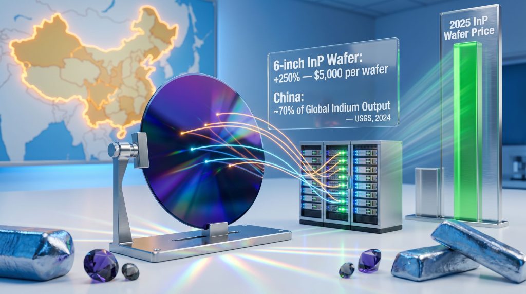
| Raw indium mining and refining | Chinese state-linked producers | Approximately 70% of global indium output (USGS, 2024) |
| InP crystal growth and substrate production | AXT (US-owned, China-based), Sumitomo (Japan), JX Advanced Metals (Japan) | AXT manufactures primarily through Chinese subsidiary |
| Wafer processing and epitaxy | Specialised fabs in US, Taiwan, Japan | Dependent on substrate supply chain |
| Optical chip fabrication | Coherent, Lumentum, VPEC, LandMark | Downstream vulnerability to substrate disruption |
| Optical module assembly | Hyperscaler supply chain integrators | End-point exposure to upstream constraints |
The critical insight here is that China's leverage operates at two distinct tiers simultaneously: raw material extraction and intermediate substrate manufacturing. This dual-layer concentration means that mining diversification alone, without accompanying processing diversification, is insufficient to resolve the underlying vulnerability. Indeed, the challenges facing rare earth processing more broadly illustrate precisely why this two-tier structure is so difficult to dismantle quickly.
China's Structural Control Over InP Supply
A 70% Production Share Is Only Part of the Story
According to the US Geological Survey's 2024 data, China accounts for approximately 70% of global indium production. Indium itself is primarily recovered as a byproduct of zinc smelting, which means new indium supply development is largely dependent on zinc mining investment decisions rather than dedicated indium projects. This byproduct dependency makes demand-driven supply expansion particularly slow to respond to price signals.
Beyond raw material production, China's influence extends directly into substrate manufacturing. AXT, the world's second-largest InP substrate producer, conducts the bulk of its manufacturing operations through its Chinese subsidiary. This creates a situation where even a US-headquartered company is subject to Chinese export licensing requirements for the substrates it physically produces inside China. AXT has publicly acknowledged the extent to which permit delays have affected its operational outlook.
This two-tier chokepoint structure has been characterised by analysts as a deliberate element of Beijing's evolving materials statecraft toolkit. Rather than imposing broad trade barriers that would invite immediate retaliation, the approach targets specific upstream compounds and substrates at points of maximum leverage, creating conditional dependencies that can be adjusted as diplomatic and commercial circumstances require.
A senior analyst at consulting firm Albright Stonebridge Group has described this approach as a granular materials chokepoint strategy, one focused on slowing or conditioning the export of the upstream compounds and substrates that determine whether the optical module ecosystem can scale at the pace required by hyperscaler demand. This framing helps explain why the InP controls are more strategically precise than Beijing's earlier rare earth restrictions, which operated at a broader elemental level.
The AXT Situation: A Case Study in Processing Geography Risk
AXT's predicament illustrates a risk category that supply chain analysts increasingly refer to as processing geography risk: the danger that manufacturing assets physically located within a jurisdiction can be subject to that jurisdiction's export control framework, regardless of the corporate ownership nationality.
AXT disclosed in May 2026 that its Chinese subsidiary did not receive its first InP export permits until June 2025, creating approximately a four-month gap from the introduction of controls in February 2025 during which unfulfilled orders accumulated into a significant backlog. The company characterised InP export permits as the most significant challenge it currently faces.
For downstream buyers such as Coherent, this translates directly into production constraints at a moment when demand for optical components is growing at extraordinary rates.
Price Signals and Market Consequences
The 250% Wafer Price Surge
The market has delivered an unambiguous signal about the severity of the supply constraint. Since China introduced formal export licensing requirements for InP in February 2025, the average price of a 6-inch InP wafer has increased by approximately 250%, rising from roughly $1,400 to approximately $5,000 per wafer.
This price escalation reflects both genuine physical supply tightness and the risk premium that buyers are now applying to a material subject to discretionary government licensing. When a government can grant or withhold export permits without a transparent or predictable timeline, buyers price in optionality accordingly.
The 250% surge in 6-inch InP wafer pricing since February 2025, from approximately $1,400 to $5,000, is not simply a supply shortfall signal. It is also a risk premium applied to a material now subject to discretionary licensing by a single regulatory authority.
The Downstream Ripple: Sold Out Through 2028
The supply disruption propagates through every layer of the optical components value chain. Lumentum, despite reportedly quadrupling its production output, has forward-sold its capacity through 2028, a booking horizon that speaks to the severity of structural undersupply relative to current demand trajectories.
Taiwanese optical component manufacturers VPEC and LandMark Optoelectronics have both experienced substrate disruptions as a direct consequence of permit delays affecting their upstream InP suppliers. In April 2026, LandMark signed a long-term InP supply agreement with Japan's Sumitomo Electric Industries, a move that reflects the urgency of securing alternative supply relationships but simultaneously compresses the pool of Sumitomo's externally available capacity for other buyers.
A research analyst at SemiAnalysis, Konrad Wang, has noted that InP is among several supply chain bottlenecks constraining the pace of AI data centre buildouts, and that the restrictions propagate through the entire optical supply chain beyond the two largest substrate producers.
The Qualification Cycle Barrier: Why Switching Suppliers Is a Multiyear Commitment
One of the least understood aspects of this supply disruption is the qualification cycle problem. In photonics manufacturing, changing substrate suppliers is not a procurement decision that can be executed through a contract amendment. It is an engineering programme.
Introducing a new InP substrate supplier requires:
- Characterising the new substrate's material properties, including crystal orientation, dislocation density, and surface roughness specifications
- Revalidating epitaxial growth processes, since different substrate lots from different manufacturers can produce meaningfully different epitaxial layer characteristics
- Running yield characterisation programmes that require substantial production volumes to generate statistically meaningful data
- Completing formal qualification approval processes, which for major photonics chipmakers serving defence or hyperscaler customers can involve additional third-party verification
These qualification cycles typically span 12 to 24 months under normal conditions. This timeline means that even if alternative InP substrate suppliers existed at sufficient scale today, the photonics manufacturers most affected by the China indium phosphide export controls could not rapidly onboard them without disrupting existing production continuity. The qualification barrier is therefore itself a mechanism that amplifies supply concentration risk.
How the Industry Is Responding
Strategic Capital Deployment Into Photonics
The investment response from major AI hardware developers has been substantial. Nvidia committed $2 billion each into Coherent and Lumentum in March 2025, signalling that optical interconnect capability has become a first-order strategic priority within the AI hardware ecosystem rather than a commodity procurement matter.
Custom chip designer Marvell Technology announced the acquisition of semiconductor startup Celestial AI to access its proprietary photonics architecture. Both moves reflect the same underlying thesis: the optical interconnect layer is the next competitive frontier in AI infrastructure, and securing that layer requires vertical integration into the photonics supply chain. Consequently, the critical minerals and semiconductors coalition forming across allied nations underscores how deeply this supply chain tension now reaches into the broader technology sector.
Domestic Capacity Expansion: The 2027 to 2028 Horizon
Coherent has announced plans to double its InP wafer manufacturing capacity at its Texas facility during 2025, with a further doubling targeted by the end of 2027. However, the capital intensity and technical complexity of InP substrate manufacturing means that new facility development typically requires two to three years from investment decision to meaningful operational output.
This timeline creates a structural gap: the supply constraint is acute now, the capacity response will not materialise at scale until 2027 at the earliest, and the demand growth curve from AI data centre expansion is not pausing to accommodate it.
The Sumitomo Constraint: Why Japan Cannot Fill the Gap Alone
Japan's Sumitomo Electric Industries has emerged as the primary alternative supplier for Western photonics manufacturers, and already holds supply relationships with Lumentum and JX Advanced Metals. However, industry sources indicate that Sumitomo consumes a substantial proportion of its InP substrate output internally, leaving insufficient external capacity to compensate for restricted Chinese exports at current demand levels.
The market leadership position is concentrated in just two players:
| Supplier | Estimated Global InP Substrate Share | Primary Constraint |
|---|---|---|
| AXT (US-owned, China-based) | ~40%+ | Subject to Chinese export licensing requirements |
| Sumitomo Electric, JX Advanced Metals (Japan) | ~40-50% combined | Primarily internal consumption; limited external availability |
| Emerging Chinese domestic players | Growing share | Export approval uncertainty; domestically oriented |
The next major ASX story will hit our subscribers first
Chinese Domestic Producers: Beneficiaries of the Controls
Rapid Capacity Scaling Among Chinese InP Manufacturers
China's export licensing regime has created a meaningful competitive advantage for domestic InP substrate producers, who can supply Chinese photonics manufacturers without restriction while overseas buyers face permit uncertainty. The leading Chinese InP substrate producers include Yunnan Germanium, Guangdong Xiandao, and Zhuhai Dingtai Xinyuan.
The scale of domestic capacity expansion is notable:
- Yunnan Germanium announced a 189 million yuan (approximately $28 million USD) investment in April 2026 targeting 450,000 single InP wafers annually, while its 2025 annual report disclosed a 74% year-on-year increase in InP wafer shipments
- Guangdong Xiandao launched a new production investment through its subsidiary Guangdong Xianrui, targeting 40 tonnes of annual InP crystal output, the raw material input for substrate manufacturing
Both companies are in discussions with Chinese authorities regarding export approvals, but industry sources indicate that any overseas shipments, if approved, are likely to be limited in volume and that near-term strategic orientation is toward domestic market supply.
Why Chinese Producers Are Not a Near-Term Solution for Western Buyers
Even setting aside the question of export approval, the qualification cycle barrier described above would prevent Western photonics manufacturers from rapidly adopting Chinese domestic producers as alternative suppliers. Established relationships between Coherent and AXT, and between Lumentum and Sumitomo, reflect years of material qualification investment that cannot be replicated quickly with new suppliers.
Geopolitical Dimensions: InP as a Diplomatic Instrument
From Trade Policy to Summit Agenda
The elevation of InP from a niche semiconductor material to an agenda item at the highest levels of US-China diplomacy is itself a remarkable development. The issue was raised during trade negotiator discussions in Seoul ahead of the May 2026 Trump-Xi summit, and formed part of the agenda carried by US business delegations accompanying the presidential visit to China. Coherent's chief executive was among those present on that delegation, specifically to address the export permit delays.
This diplomatic salience reflects a broader pattern in Beijing's approach to economic statecraft. The InP controls follow the structural logic of earlier restrictions on gallium and germanium introduced in 2023, and represent an incremental refinement of that approach toward more precise, application-specific targeting. In addition, China's bismuth export controls reveal a similarly calibrated pattern of targeting materials at points of maximum downstream dependency.
The strategic logic is asymmetric: imposing restrictions on a specific upstream compound creates leverage over an entire downstream technology ecosystem without triggering the same breadth of immediate retaliation as a broad trade barrier would. The conditionality of export licensing, as opposed to an outright ban, preserves diplomatic flexibility while creating ongoing uncertainty that itself functions as a constraint on investment and planning.
Long-Term Resilience Strategies and Their Limitations
Upstream Mining Diversification
Because indium is primarily a byproduct of zinc smelting, developing new indium supply is structurally dependent on zinc mining investment decisions. Geographic diversification of indium refining capacity exists in Canada, South Korea, and Belgium, but expanding that capacity requires multi-year investment horizons and is not responsive to near-term demand signals from the photonics sector alone.
Photonic Architecture Evolution
A longer-term response involves rearchitecting photonic systems to reduce InP dependency for certain functions. Silicon photonics offers a partial pathway for lower-specification interconnect applications, and some AI hardware developers are exploring hybrid architectures that reserve InP for the highest-performance optical functions while deploying silicon photonics more broadly.
However, these architectural transitions require their own multi-year development and qualification cycles, and involve accepting performance trade-offs that are material at the compute densities required by frontier AI model training.
The InP situation reveals a structural asymmetry in the global AI supply chain: while model development and chip design are geographically distributed, the upstream materials chains that enable AI hardware manufacturing remain highly concentrated, and that concentration is now being actively leveraged as a policy instrument.
The defence and critical minerals supply chain crisis emerging across allied nations is, in many respects, the broader strategic context within which the China indium phosphide export controls must be understood.
Frequently Asked Questions
What is indium phosphide used for in AI data centres?
Indium phosphide is the primary substrate material used to fabricate high-speed optical lasers and photodetectors. These components form the photonic interconnect layer in AI data centres, enabling fibre-optic data transmission at the bandwidth and energy efficiency levels required by large-scale AI training and inference workloads.
Why does China have so much control over indium phosphide supply?
China accounts for approximately 70% of global indium production and hosts significant InP substrate manufacturing capacity, including the primary production operations of the world's second-largest substrate producer. This concentration at both the raw material and processing stages provides Beijing with substantial leverage over global InP supply.
How much have InP wafer prices increased since China's export controls began?
Since China introduced export licensing requirements for InP in February 2025, the average price of a 6-inch InP wafer has risen by approximately 250%, reaching around $5,000 per wafer.
Can AI data centres use alternative materials instead of indium phosphide?
No commercially scalable substitute currently matches InP's performance in high-speed optical applications. Silicon photonics offers a partial alternative for lower-specification interconnect functions, but InP remains essential for the highest-performance photonic components used in AI infrastructure.
How long will it take to build alternative InP substrate supply outside China?
New InP substrate manufacturing facilities typically require two to three years from investment decision to meaningful operational capacity. Diversification away from Chinese-controlled production is therefore unlikely to deliver material supply relief before 2028.
What is the qualification cycle and why does it matter?
The qualification cycle is the engineering validation process required before a photonics manufacturer can use substrates from a new supplier. It typically spans 12 to 24 months and involves extensive material characterisation, process revalidation, and yield testing. This barrier prevents rapid supplier switching even when alternative sources theoretically exist.
Key Takeaways
- China controls approximately 70% of global indium production and hosts critical InP substrate manufacturing capacity, creating a two-tier supply chain chokepoint at both the raw material and processing stages
- Export licensing requirements introduced in February 2025 have driven a 250% price increase in 6-inch InP wafers, reaching approximately $5,000 per wafer
- The disruption propagates through the entire photonics value chain, with Lumentum's order book sold out through 2028 despite quadrupling production output
- Alternative supply from Sumitomo is constrained by substantial internal consumption, while new domestic US capacity at facilities such as Coherent's Texas plant will not reach meaningful scale before 2027
- Chinese domestic producers, including Yunnan Germanium targeting 450,000 wafers annually, are scaling rapidly but remain primarily oriented toward domestic supply
- The qualification cycle barrier of 12 to 24 months prevents rapid supplier switching, materially amplifying the impact of any supply disruption on photonics manufacturers
- InP has achieved genuine diplomatic salience, featuring directly in US-China trade negotiations at summit level, reflecting its structural importance to the global AI infrastructure buildout
Disclaimer: This article contains forward-looking analysis and references to market forecasts. These projections involve inherent uncertainty and should not be construed as investment advice. Readers are encouraged to consult independent financial and industry research before making investment decisions.
Want to Stay Ahead of the Critical Minerals Driving the Next Wave of ASX Discoveries?
The supply chain tensions reshaping global AI infrastructure highlight just how consequential upstream mineral positions can become — and Discovery Alert's proprietary Discovery IQ model delivers real-time alerts the moment significant ASX mineral discoveries are announced, turning complex commodity data into actionable investment insights. Explore historic discoveries and their remarkable market returns, then start your 14-day free trial at Discovery Alert to ensure you're positioned ahead of the broader market when the next major find is made.