
July 13, 2026
What Are Japan's New Semiconductor Export Controls and Why Do They Matter?
Japan semiconductor export controls represent a fundamental shift in how the nation approaches technology trade policy, significantly impacting global semiconductor supply chains. These restrictions target the most advanced segments of chip manufacturing, creating potential bottlenecks for countries seeking to develop cutting-edge semiconductor capabilities. The strategic implications extend far beyond traditional trade relationships, reflecting broader US‑China trade war strategies that have reshaped international technology governance.
Understanding METI's Expanded Licensing Framework Under FEFTA
The Ministry of Economy, Trade and Industry implemented comprehensive controls in March 2023, targeting 23 categories of semiconductor manufacturing equipment under the Foreign Exchange and Foreign Trade Act. This regulatory approach allows Japanese authorities to scrutinise exports of dual-use technologies that could contribute to military applications or compromise international security.
The licensing system requires manufacturers to obtain METI approval before shipping controlled items to specific destinations or end-users. This framework provides significant discretionary power to Japanese regulators, who can adjust approval rates and processing timelines based on evolving geopolitical circumstances.
The 33-Category Equipment Control System Explained
Japan's control regime encompasses sophisticated manufacturing tools essential for producing advanced semiconductors. The restrictions cover extreme ultraviolet lithography systems, plasma etching equipment for high-aspect-ratio structures, and atomic layer deposition tools capable of creating films thinner than 10 nanometres.
These controls specifically target equipment used in manufacturing chips at 14nm and below, effectively limiting access to technologies required for cutting-edge processor and memory production. The technical thresholds align with similar restrictions implemented by allied nations, creating coordinated pressure on targeted countries.
Timeline of Implementation: From March 2023 to January 2025 Proposals
The evolution of Japan semiconductor export controls demonstrates escalating technological competition. Initial restrictions focused on traditional semiconductor equipment, while proposed January 2025 expansions would encompass electronic design automation software and additional testing equipment.
These proposed expansions would target design tools for nodes below 14nm, simulation software for 3D chip stacking, and reliability testing systems for advanced packaging. The inclusion of software controls represents a significant broadening beyond physical equipment restrictions.
When big ASX news breaks, our subscribers know first
Which Critical Technologies Fall Under Japan's Export Restrictions?
Japan's export controls target technologies across the entire semiconductor manufacturing ecosystem, from initial design software to final testing equipment. This comprehensive approach affects multiple stages of chip production, creating potential disruptions throughout global supply chains. Furthermore, these measures complement broader Trump tariff implications for international technology trade.
Advanced Lithography and Etching Equipment Controls
Deep ultraviolet immersion lithography systems capable of producing chips at 14nm and below face strict export licensing requirements. These systems, essential for creating the intricate patterns that define modern semiconductor architectures, represent some of the most sophisticated manufacturing tools available globally.
Extreme ultraviolet lithography equipment, operating at 13.5nm wavelength, falls under the most restrictive categories. Only a handful of companies worldwide possess the technical capability to produce these systems, making export controls particularly impactful for countries seeking advanced manufacturing capabilities.
Deposition, Cleaning, and Thermal Processing Tool Restrictions
Chemical vapour deposition and atomic layer deposition equipment designed for advanced node production requires export licenses. These tools create the multiple layers of materials that comprise modern semiconductors, with precision requirements measured in individual atomic layers.
Cleaning equipment for removing contaminants during manufacturing processes also faces restrictions. The ultra-pure environments required for advanced chip production depend on specialised cleaning systems that maintain contamination levels below parts-per-trillion thresholds.
Front-End Testing and Measurement Equipment Limitations
Proposed expansions would encompass wafer probe stations capable of testing advanced logic and memory devices. Final test equipment for chips operating above 3 GHz would require additional licensing, affecting access to tools needed for validating high-performance processors.
How Does Japan's Photoresist Market Dominance Create Strategic Leverage?
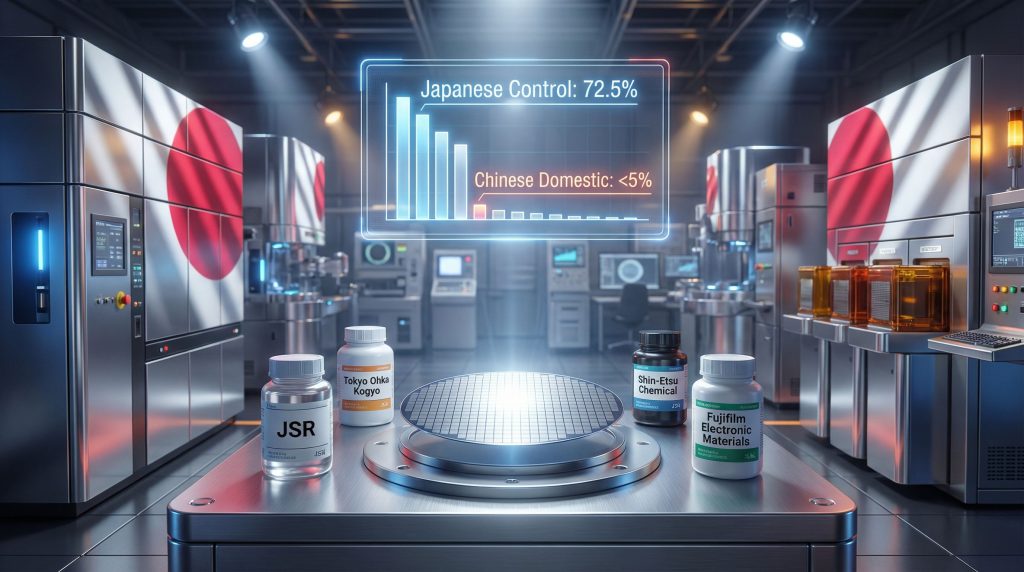
Japan's control over photoresist chemicals represents one of the most concentrated supply chain dependencies in semiconductor manufacturing. These light-sensitive materials, essential for creating the microscopic patterns that define chip architectures, cannot be easily substituted or rapidly sourced from alternative suppliers. However, geopolitical tensions may lead to broader critical minerals executive order initiatives affecting related supply chains.
The Big Four: JSR, Tokyo Ohka Kogyo, Shin-Etsu Chemical, and Fujifilm's Market Control
| Company | Country | Market Share | Specialisation |
|---|---|---|---|
| JSR | Japan | ~25% | Advanced EUV resists |
| Tokyo Ohka Kogyo | Japan | ~20% | ArF immersion resists |
| Shin-Etsu Chemical | Japan | ~15% | Multi-layer resist systems |
| Fujifilm Electronic Materials | Japan | ~12.5% | Next-gen materials |
| Combined Japanese Control | – | 72.5% | – |
| Chinese Domestic Production | China | <5% | Basic photoresists |
This market concentration reflects decades of specialised research and development investment. Japanese companies have maintained technological leadership through continuous innovation in photochemistry, developing materials that can achieve resolution capabilities below 20nm with extreme sensitivity to ultraviolet light.
Why Chinese Semiconductor Fabs Remain Critically Dependent on Japanese Chemicals
Chinese domestic photoresist production remains concentrated in basic materials suitable for mature manufacturing nodes. Companies like Beijing Kehua Microelectronics produce argon fluoride photoresists for 90nm-65nm applications, while advanced EUV-compatible materials remain beyond current Chinese technological capabilities.
The technology gap between Chinese and Japanese photoresist suppliers spans an estimated 7-10 years for advanced node applications. This disparity reflects the complex chemistry and precise manufacturing requirements for materials operating at the extremes of physical and chemical performance.
Technical Barriers to Photoresist Substitution and Localisation Challenges
Developing advanced photoresist materials requires extensive knowledge of polymer chemistry, optical physics, and semiconductor device architecture. The interaction between photoresist properties and lithographic exposure systems creates system-level dependencies that cannot be easily replaced through simple material substitution.
Qualification processes for new photoresist materials can extend 18-24 months, involving comprehensive testing across multiple manufacturing conditions and device architectures. This lengthy validation timeline creates significant barriers to rapid supply chain diversification.
What Strategic Scenarios Could Emerge from Escalating Trade Tensions?
Multiple pathways exist for escalating technological restrictions, each carrying distinct implications for global semiconductor manufacturing and geopolitical relationships. These scenarios range from incremental tightening to comprehensive technology embargoes. Additionally, global tariff impacts may accelerate technological decoupling processes.
Scenario 1: Graduated Export Licence Restrictions
Licensing systems can be calibrated to target specific end-users or applications while maintaining general trade flows. This approach, similar to the US Entity List model, would allow selective restrictions on particular companies or technologies while preserving broader economic relationships.
Graduated restrictions might focus on advanced military applications while permitting civilian semiconductor production. However, the dual-use nature of semiconductor technologies complicates clear distinctions between military and civilian applications.
Scenario 2: Complete Photoresist Export Suspension
A comprehensive photoresist embargo would create immediate disruptions for Chinese semiconductor manufacturers operating advanced production nodes. Given the concentrated supply base and lengthy qualification requirements, alternative sourcing options remain extremely limited.
Such restrictions would likely trigger significant Chinese retaliation through controls on critical materials where Beijing maintains market dominance, including rare earth elements, gallium, and germanium. China controls 60% of global rare earth mining and 85% of processing capacity.
Scenario 3: Coordinated Allied Technology Embargo
Multilateral restrictions coordinated through frameworks like the Wassenaar Arrangement would create comprehensive barriers to advanced semiconductor technology transfer. This scenario would align Japanese, American, Dutch, and European export controls to eliminate alternative sourcing pathways.
Japan's control over semiconductor manufacturing chemicals represents one of the most concentrated chokepoints in the global tech supply chain. Unlike equipment, which can sometimes be sourced from multiple vendors, photoresist chemistry requires years of R&D investment and cannot be easily substituted.
Which Chinese Semiconductor Companies Face the Greatest Exposure?
Chinese semiconductor manufacturers vary significantly in their vulnerability to Japan semiconductor export controls, depending on their technological ambitions and current manufacturing capabilities. Companies pursuing advanced node production face the highest exposure levels. In addition, China's export controls strategy demonstrates Beijing's potential for retaliatory measures.
SMIC's Advanced Node Production Vulnerabilities
Semiconductor Manufacturing International Corporation operates fabs at 14nm and attempts 7nm production, placing it directly within the scope of Japanese export controls. The company's Q3 2023 revenue reached $1.63 billion, with capital expenditure of $6.5 billion annually supporting ambitious expansion plans.
SMIC's advanced node development relies heavily on imported equipment and materials from Japanese suppliers. Disruptions to this supply chain would significantly impact the company's ability to compete with international foundries like TSMC and Samsung.
Memory Manufacturers: YMTC and CXMT Risk Assessment
Yangtze Memory Technologies Corporation achieved 232-layer 3D NAND production in 2023, representing significant technological progress. However, this advancement depends on sophisticated equipment and materials from Japanese suppliers, creating vulnerability to export restrictions.
ChangXin Memory Technologies produces DRAM memory with current capacity of 40,000 wafers per month. The company successfully manufactures DDR4 and LPDDR4X memory, but advanced node development for next-generation products requires continued access to Japanese materials and equipment.
Foundry Operations: Hua Hong and Huali Microelectronics Dependencies
| Company | Primary Business | Japanese Equipment Dependency | Risk Level |
|---|---|---|---|
| SMIC | Logic foundry | High (advanced nodes) | Critical |
| YMTC | 3D NAND memory | Very High | Critical |
| CXMT | DRAM memory | High | Severe |
| Hua Hong | Specialty foundry | Moderate-High | Significant |
| Huali Micro | RF/analog chips | Moderate | Moderate |
Specialty foundries face varied exposure levels depending on their technology focus. Radio frequency and analogue chip production generally requires less advanced manufacturing processes, reducing vulnerability to export controls targeting cutting-edge technologies.
How Do Japan's Controls Compare to US and Dutch Export Restrictions?
International coordination on semiconductor export controls creates overlapping restrictions that reinforce each other while addressing different aspects of the technology supply chain. These coordinated efforts represent unprecedented cooperation in technology trade policy.
Coordination vs. Independence in Allied Export Control Strategy
The United States implemented comprehensive semiconductor export controls in October 2022, targeting China's access to advanced chips and manufacturing equipment. Dutch restrictions focus specifically on advanced deep ultraviolet lithography systems from ASML, whilst Japanese controls emphasise materials and processing equipment.
This division of regulatory focus reflects each country's industrial strengths and supply chain positions. American controls leverage dominance in chip design tools and advanced processors, Dutch restrictions capitalise on lithography equipment leadership, and Japanese measures exploit materials and equipment advantages.
Technical Scope Differences Between National Approaches
US controls target production capabilities at 14nm/16nm and below for logic chips, while Dutch controls focus on DUV systems capable of 28nm and below with immersion lithography. Japan semiconductor export controls cover equipment for 14nm and below plus critical materials across all manufacturing nodes.
The global EDA software market, valued at $13.1 billion in 2023, remains primarily under US control through companies like Synopsys, Cadence, and Mentor/Siemens. Japanese proposed expansions into EDA controls would complement rather than duplicate American restrictions.
Licensing Procedures: Simplified Access for Wassenaar Arrangement Countries
The Wassenaar Arrangement, encompassing 42 participating states, provides frameworks for multilateral export control coordination. Japan, the United States, and Netherlands leverage this structure to align their restrictions whilst maintaining preferential access for allied nations.
Licensing procedures generally provide expedited approval for exports to allied countries while imposing heightened scrutiny for shipments to strategic competitors. This approach maintains alliance solidarity whilst targeting specific geopolitical concerns.
The next major ASX story will hit our subscribers first
What Are the Proposed January 2025 Control Expansions?
Japan's proposed regulatory expansions would significantly broaden the scope of semiconductor export controls beyond manufacturing equipment to encompass design software and additional testing capabilities. These measures reflect evolving understanding of technology supply chain vulnerabilities.
EDA Software and CAD Tool Restrictions
Electronic Design Automation software controls would target advanced design tools including layout design software for nodes below 14nm, simulation tools for 3D chip stacking and advanced packaging, and design rule checking systems.
Three major companies control approximately 75% of the global EDA market, with US firms maintaining dominant positions. Japanese restrictions would complement American controls by targeting specific software categories and versions used in advanced chip design.
Enhanced Testing and Measurement Equipment Controls
Proposed testing equipment restrictions would encompass wafer probe stations capable of testing advanced logic and memory devices, final test equipment for chips operating above 3 GHz, and reliability testing systems for advanced packaging applications.
These controls would affect the validation and quality assurance processes essential for advanced semiconductor production. Testing equipment restrictions could create bottlenecks even when manufacturing equipment remains available.
Direct Semiconductor Component Export Limitations
Some proposals include restrictions on direct semiconductor component exports, particularly for chips with potential military or strategic applications. This approach would extend controls beyond manufacturing capabilities to finished products.
Could Japan's Semiconductor Leverage Backfire Economically?
Export restrictions carry significant economic risks for Japanese manufacturers who depend heavily on Chinese markets for revenue and growth. These trade dependencies create complex strategic calculations balancing geopolitical objectives with commercial interests.
Revenue Impact on Japanese Equipment and Chemical Manufacturers
Japanese semiconductor equipment exports to China totalled ¥972 billion ($7.2 billion) in 2022, representing 25.3% of total Japanese semiconductor equipment exports. Major manufacturers face substantial revenue exposure to Chinese market restrictions.
- Tokyo Electron: China sales represented 24% of total revenue in FY2022
- Screen Holdings: China sales approximately 30% of semiconductor equipment revenue in 2022
These dependencies create internal industry pressure against comprehensive export restrictions that could eliminate or substantially reduce Chinese market access.
Potential Chinese Retaliation Through Rare Earth and Critical Mineral Access
China maintains dominant positions in critical materials essential for Japanese manufacturing industries. Beijing controls 85% of rare earth processing capacity and produces 80% of global natural graphite essential for lithium-ion batteries.
The December 2023 implementation of Chinese export controls on gallium and germanium demonstrates Beijing's willingness to weaponise material dependencies. Japan imports approximately 40% of its gallium from China, creating vulnerability to supply disruptions.
Chinese dominance extends to processing of cobalt (73%), lithium (59%), and manganese (93%), providing multiple leverage points for potential retaliation against Japanese technology restrictions.
Long-Term Market Share Risks from Accelerated Chinese Substitution Efforts
Export restrictions may accelerate Chinese domestic development programmes designed to achieve supply chain independence. China's National IC Industry Investment Fund Phase III, announced in 2024, exceeds 300 billion yuan ($42 billion) in expected funding.
Historical precedents suggest that trade restrictions can successfully motivate technological substitution over extended timeframes. Japan's own response to the 2010 Chinese rare earth export restrictions reduced consumption by 30% through alternative materials and supply diversification.
What Alternative Supply Chain Strategies Are Available to Chinese Manufacturers?
Chinese semiconductor companies possess multiple strategies for mitigating export restrictions, ranging from short-term inventory management to long-term technological development programmes. The effectiveness of these approaches varies significantly across different technology categories.
Stockpiling and Strategic Inventory Management
Evidence suggests Chinese manufacturers increased semiconductor equipment imports by 15% year-over-year in the first half of 2023, before additional controls took effect. Photoresist imports from Japan increased 22% in Q1 2023 compared to Q1 2022, indicating anticipatory stockpiling.
Strategic inventory accumulation can provide temporary buffers against supply disruptions, but storage limitations and material degradation constrain long-term effectiveness. Photoresist chemicals have limited shelf lives, requiring careful inventory rotation and management.
Domestic R&D Investment Acceleration Programmes
Chinese government semiconductor investment through the National IC Industry Investment Funds demonstrates substantial financial commitment to achieving technological independence. Combined phases of funding exceed $70 billion in government-directed investment.
Domestic photoresist development efforts include Beijing Kehua Microelectronics producing ArF photoresists for 90nm-65nm nodes and Nanda Optoelectronic Material developing i-line and KrF photoresists. However, the technology gap for advanced nodes remains substantial.
Third-Country Sourcing and Transshipment Possibilities
Alternative sourcing through third countries may provide limited relief for some materials and equipment. However, the concentrated nature of advanced semiconductor supply chains limits effective alternative suppliers for critical components.
End-use verification requirements and know-your-customer obligations create compliance challenges for third-country sourcing strategies. Export control regimes increasingly focus on preventing circumvention through transshipment arrangements.
How Might This Reshape Global Semiconductor Manufacturing Geography?
Export restrictions could accelerate geographic redistribution of semiconductor manufacturing capacity as companies seek to minimise supply chain vulnerabilities. These shifts may create new regional production clusters whilst reducing concentration in traditional manufacturing centres.
Potential Fab Relocation to Southeast Asian Markets
Southeast Asian countries offer potential alternatives for semiconductor manufacturing expansion, providing access to both Chinese and international markets whilst maintaining some distance from direct geopolitical tensions.
Countries like Malaysia, Thailand, and Vietnam possess established electronics manufacturing ecosystems and could potentially host expanded semiconductor assembly and test operations. However, advanced fabrication requires extensive infrastructure investments and skilled workforce development.
Investment Shifts Toward Non-Aligned Technology Suppliers
Export restrictions may create market opportunities for technology suppliers from countries not participating in coordinated control regimes. South Korean, Taiwanese, and European companies could benefit from reduced Japanese and American competition in restricted markets.
However, the technical complexity of advanced semiconductor manufacturing limits the number of viable alternative suppliers. Many critical technologies remain concentrated among a small number of global leaders regardless of their national origins.
Emergence of Parallel Semiconductor Ecosystems
Prolonged trade restrictions could facilitate the development of parallel technology ecosystems with limited interconnection. Chinese domestic suppliers might achieve sufficient capabilities to serve domestic markets whilst international suppliers focus on unrestricted countries.
This bifurcation would reduce global efficiency and increase development costs across both ecosystems, as economies of scale diminish and redundant R&D investments increase.
What Are the Long-Term Implications for Global Tech Competition?
The intersection of Japan semiconductor export controls with broader technological competition creates long-term structural changes in global innovation systems. These developments extend far beyond immediate trade relationships to fundamental questions about technological sovereignty and international cooperation.
Acceleration of Technology Decoupling Between East and West
Semiconductor restrictions represent one component of broader technological decoupling between major powers. Export controls create incentives for developing independent technology stacks that minimise dependencies on potentially hostile suppliers.
This decoupling process extends beyond semiconductors to encompass artificial intelligence, quantum computing, biotechnology, and renewable energy technologies. The semiconductor industry serves as a template for similar restrictions across multiple technology domains.
Impact on AI and Advanced Computing Development Timelines
Advanced artificial intelligence applications depend critically on cutting-edge semiconductor capabilities for training large language models and implementing real-time inference. Export restrictions on advanced chips and manufacturing equipment could significantly impact AI development timelines.
Countries with restricted access to advanced semiconductors may need to develop alternative approaches to AI computation, potentially emphasising efficiency optimisation over raw computational power. These alternative pathways could yield innovative approaches to AI development.
Strategic Implications for Taiwan's Semiconductor Industry Position
Taiwan's dominant position in advanced semiconductor manufacturing creates unique strategic dynamics as export restrictions reshape global supply chains. TSMC's technological leadership provides significant leverage whilst creating potential vulnerabilities.
Export controls that limit Chinese access to advanced manufacturing could benefit Taiwanese foundries by redirecting demand to unrestricted suppliers. However, geopolitical tensions surrounding Taiwan create ongoing risks for global supply chain stability.
Furthermore, developments regarding Japan's semiconductor export controls demonstrate how technological capabilities increasingly intersect with national security considerations, representing one element of a broader transformation in global technology governance that prioritises strategic competition alongside traditional economic efficiency.
Are You Ready to Capitalise on Japan's Semiconductor Export Controls?
Japan's semiconductor export restrictions present significant opportunities for investors tracking global technology supply chains and geopolitical shifts. Discovery Alert's proprietary Discovery IQ model delivers real-time alerts on ASX mineral discoveries, including critical materials like rare earth elements and lithium that are increasingly vital for semiconductor manufacturing and technology independence – begin your 30-day free trial today to position yourself ahead of these transformative market dynamics.