

July 7, 2026
The Physics Problem That Killed Tungsten's Dominance in Memory Chips
Every major materials transition in semiconductor manufacturing begins the same way: not with a discovery, but with a ceiling. Engineers push an existing material further, observe diminishing returns, and eventually confront an uncomfortable truth that the physics simply will not cooperate any further. That is precisely what has happened with tungsten in 3D NAND flash memory, and the resulting shift toward molybdenum is now reshaping both the semiconductor supply chain and the global minor metals market in ways that few outside the industry fully appreciate.
Understanding why molybdenum replacing tungsten in NAND flash chips has become one of the most consequential materials transitions in advanced memory manufacturing requires starting at the atomic scale, not the commodity market. Furthermore, tungsten's strategic importance across multiple industries makes this substitution all the more significant to track.
When big ASX news breaks, our subscribers know first
How Tungsten Became the Default and Why That Era Is Ending
Tungsten earned its place in semiconductor fabrication through an impressive combination of thermal stability, relatively low bulk resistivity, and mature deposition chemistry. For roughly two and a half decades, it served as the standard interconnect and word-line metal across NAND architectures. Its melting point of 3,422°C made it practically indestructible under the thermal budgets imposed during chip fabrication, and foundries developed highly refined tungsten fluoride (WF₆) chemical vapour deposition processes that were reliable at scale.
The problem is that tungsten's performance is strongly geometry-dependent. In bulk form, its resistivity characteristics are acceptable. However, as device dimensions compress into the nanoscale regime and 3D NAND stacks extend vertically beyond 300 layers, tungsten's resistivity escalates sharply in thin-film configurations. This phenomenon, driven by increased electron scattering at grain boundaries and surfaces, translates directly into slower signal transmission and higher power consumption — two outcomes fundamentally incompatible with next-generation memory architecture requirements.
The second compounding issue is what engineers call RC delay: the product of resistance (R) and capacitance (C) that governs how quickly a signal can propagate through a conductor. As word-line geometries shrink in ultra-high-stack memory designs, RC delay becomes a performance bottleneck. Tungsten's worsening thin-film resistivity makes this problem progressively harder to manage with conventional design solutions.
There is also a contamination dimension that receives far less attention outside fabrication circles. Tungsten deposition using WF₆ precursors introduces fluorine into the fabrication environment. Fluorine contamination is notoriously difficult to control at the feature sizes relevant to advanced NAND, and it contributes to dielectric degradation and leakage failures over time.
What Makes Molybdenum Technically Superior in Advanced 3D NAND
Molybdenum does not replace tungsten because it is inherently a better metal in absolute terms. It replaces tungsten because it behaves better under the specific constraints imposed by ultra-scaled 3D NAND fabrication. This distinction matters enormously for understanding the scope and limits of the substitution story.
Resistivity at Nanoscale: The Core Differentiator
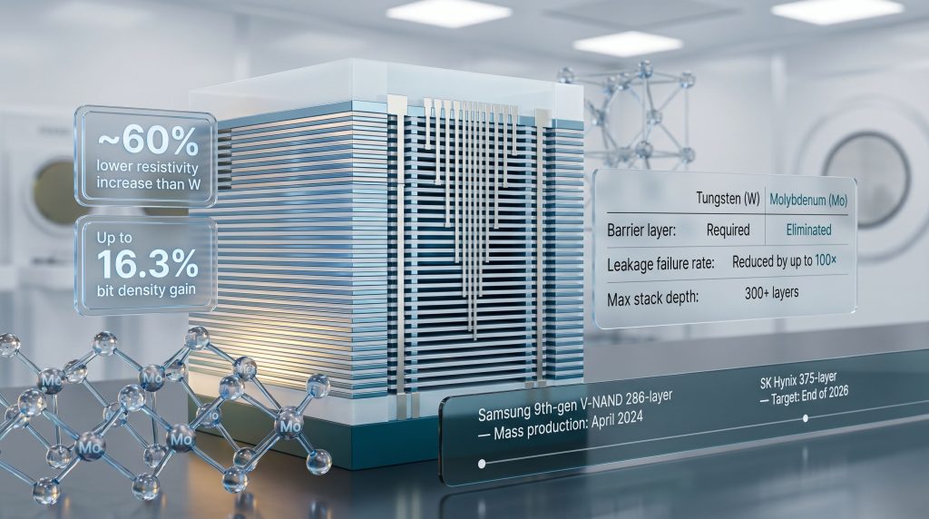
At nanoscale dimensions, molybdenum exhibits approximately 60% less resistivity increase than tungsten in thin-film configurations. This is not a marginal improvement. In a technology domain where engineers measure progress in single-digit percentage gains, a 60% reduction in thin-film resistivity degradation represents a genuinely transformative advantage. Faster signal propagation, lower power draw, and improved device reliability all follow from this single material property.
The Barrier Layer Elimination Advantage
One of the less obvious but structurally important advantages of molybdenum involves barrier layer requirements:
- Tungsten deposition requires a dedicated barrier layer, typically titanium nitride (TiN), to prevent metal diffusion into surrounding dielectric materials
- This barrier layer consumes valuable cross-sectional area within each word-line feature that could otherwise carry current
- Molybdenum's material properties permit barrier-free deposition in certain NAND architectures, recovering that lost cross-section for full current-carrying capacity
- The practical result is higher effective conductivity within an identical physical space, enabling denser cell packing without increasing feature dimensions
Fluorine-Free Deposition and Leakage Reduction
Molybdenum can be deposited using fluorine-free precursor chemistries, eliminating the contamination risk associated with WF₆-based tungsten processes. Industry research has demonstrated that this single change can reduce leakage failure rates by up to 100 times compared to tungsten-based word-line designs. For memory manufacturers where yield is the primary economic lever, a leakage failure reduction of this magnitude is commercially decisive.
Research published by Kioxia has validated that wordline pitch reduction enabled by molybdenum can deliver a 7.3% reduction in wordline pitch and bit density gains of up to 16.3% — a result that directly translates into more storage per unit area and lower cost per gigabyte across the product stack.
Molybdenum vs. Tungsten in 3D NAND: Full Technical Comparison
| Performance Parameter | Tungsten (W) | Molybdenum (Mo) |
|---|---|---|
| Resistivity behaviour at nanoscale | Increases sharply in thin films | ~60% lower increase than W |
| Barrier layer requirement | Required (reduces usable cross-section) | Eliminated (full cross-section utilised) |
| Fluorine contamination risk | High (WF₆ precursor-based deposition) | Eliminated via fluorine-free precursors |
| Leakage failure rate | Baseline | Reduced by up to 100× |
| Maximum viable stack depth | ~300 layers (physical ceiling) | Supports 300+ layer architectures |
| Bit density improvement | Baseline | Up to 16.3% gain via pitch shrink |
| Melting point | 3,422°C | 2,623°C (sufficient for NAND thermal budgets) |
| Scalability for GAA logic | Limited | Applicable to gate-all-around architectures |
Which Chipmakers Are Leading the Molybdenum Transition
The commercial adoption timeline for molybdenum in NAND fabrication has moved faster than many observers anticipated, with multiple major manufacturers now at different stages of the transition.
| Manufacturer | Technology Node / Generation | Key Milestone | Production Timeline |
|---|---|---|---|
| Samsung | 9th-gen V-NAND (286-layer) | First commercial Mo word-line adoption | Mass production: April 2024 |
| SK Hynix | 375-layer 3D NAND | Design verification completed; Mo replaces W in word lines | Mass production target: End of 2026 |
| Kioxia | Advanced NAND research | Demonstrated 7.3% wordline pitch reduction and 16.3% bit density gain with Mo | Published research findings |
| Micron | High-volume NAND | Early Mo adoption via Lam Research ALTUS Halo ALD tooling | High-volume production: 2025+ |
Samsung's entry into mass production of its ninth-generation V-NAND at 286 layers in April 2024 using molybdenum in metal gate word-line applications represented the first commercial-scale proof point for the transition. SK Hynix's June 2026 announcement of design verification on its 375-layer 3D NAND architecture using molybdenum was the catalyst that sparked a significant rally in molybdenum-related equities, including Jinduicheng Molybdenum Co. reaching a 16-year share price high of 31.61 yuan per share on the Shanghai Stock Exchange on June 23, 2026, according to Fastmarkets reporting.
A Samsung semiconductor process engineer confirmed to Fastmarkets that many NAND flash manufacturers have been replacing tungsten with molybdenum in metal gate applications, and expressed the expectation that next-generation NAND flash devices would increasingly adopt molybdenum gates over the coming years, until a further alternative material is identified.
The Equipment Dimension: Why Lam Research's ALTUS Halo Matters
Materials transitions in semiconductor manufacturing do not happen through chemistry alone. Deposition tooling is the operational gatekeeper. Lam Research's ALTUS Halo atomic layer deposition (ALD) system has been cited as a key enabler of molybdenum adoption, with the platform demonstrating greater than 50% word-line resistance reduction compared to tungsten-based processes. The availability, qualification, and capacity of such specialised ALD equipment will meaningfully influence how quickly the broader industry can accelerate adoption beyond the early movers.
Tungsten Price Volatility: The Commercial Accelerant
While the technical case for molybdenum replacing tungsten in NAND flash chips was established in research settings well before commercial adoption, procurement teams require commercial motivation to act. Tungsten's extraordinary price volatility between 2025 and 2026 provided exactly that motivation. In addition, the broader critical minerals demand surge across advanced manufacturing has intensified scrutiny of supply chain dependencies at every level.
Fastmarkets' weekly price assessment for tungsten concentrate (65% WO₃, in-warehouse China) reached a record high of 1,025,000 yuan per tonne at the midpoint on March 11, 2026. By July 1, 2026, that same assessment had retreated to 495,000 yuan per tonne — a decline of more than 50% from its peak within a matter of months.
This type of extreme price swing, from record highs to a halving of value within a single year, creates an almost impossible procurement planning environment. For chipmakers operating at scale, where materials costs directly affect cost-per-bit economics, this kind of volatility is precisely the trigger that accelerates substitution conversations.
Industry sources have confirmed that cost considerations move to the forefront of chipmaker decision-making whenever tungsten prices surge dramatically, and that the 2025–2026 cycle materially intensified discussions around molybdenum as an alternative. Consequently, tungsten offtake agreements have also come under renewed scrutiny as buyers reassess long-term procurement strategies.
The next major ASX story will hit our subscribers first
Molybdenum Market Structure: Why Semiconductor Demand Is Strategic, Not Transformative
Understanding the commodity market implications of this transition requires an accurate picture of molybdenum's existing demand structure. Steel alloying accounts for approximately 80% of global molybdenum consumption, where the metal is used as an addition in stainless, specialty, and high-strength steels. China is simultaneously the world's largest producer and consumer of molybdenum.
Against this backdrop, a Japan-based molybdenum trader confirmed to Fastmarkets that near-term incremental semiconductor demand for molybdenum is estimated at approximately 80 tonnes. To contextualise that figure against the scale of global molybdenum markets, annual global molybdenum production runs into hundreds of thousands of tonnes. Semiconductor applications are, therefore, a high-value demand category but not a near-term volume shock.
The more accurate characterisation is that semiconductor adoption of molybdenum represents a demand diversification story rather than a demand transformation story. It links the metal's demand profile to semiconductor and AI investment cycles for the first time, gradually reducing its near-total dependence on steel sector dynamics.
This strategic linkage carries its own significance for longer-term market positioning, even if the volume numbers remain modest in the near term.
Molybdenum Prices and Current Supply Tightness
Independent of the semiconductor narrative, molybdenum prices have been supported by genuine fundamental tightness. Fastmarkets' daily price assessment for molybdenum MB drummed molybdic oxide (Mo, in-warehouse Busan) reached a high not seen in over three years at $31.45 per lb at the midpoint on May 12, 2026, and continued to hover at elevated levels into early July 2026.
Supply constraints stem from multiple sources:
- Permitting delays and extended timelines for bringing new molybdenum mining projects into production
- Limited incremental output growth from existing concentrate producers
- Steadily growing stainless steel sector demand providing a persistent consumption floor
- A globally concentrated production base that limits supply-side responsiveness to price signals
The Supply Pipeline: New Mines From 2028
Two major Chinese projects are expected to materially alter the supply outlook from 2028 onward, providing a medium-term counterweight to current tightness.
Caosiyao: Inner Mongolia
| Project Parameter | Detail |
|---|---|
| Location | Inner Mongolia, northern China |
| Total ore resource | 1.035 billion tonnes |
| Contained molybdenum | 1.089 million tonnes |
| Total investment | ~10 billion yuan |
| Mining method | Open-pit and underground combined |
| Annual ore processing capacity | 16.5 million tonnes |
| Mine life | 81 years |
| Production start | 2028 (scheduled) |
Shapinggou: Anhui Province
| Project Parameter | Detail |
|---|---|
| Location | Jinzhai County, Anhui Province, eastern China |
| Proven recoverable molybdenum metal | 2.10 million tonnes |
| Global ranking | Second-largest molybdenum mine by resource |
| Owner | Zijin Mining Group (majority) |
| Development stage | Beneficiation project construction commenced June 2026 |
| Production start | 2028 (scheduled) |
Beyond China, major copper-molybdenum operations in North and South America are also planning output increases. Together, these supply expansions are expected to ease current market tightness and moderate price support across the 2028–2030 timeframe, creating a two-phase market dynamic: near-term tightness supporting prices, followed by medium-term supply relief.
The High-Purity Processing Bottleneck: The Real Competitive Barrier
One insight that is frequently overlooked in commodity-level analysis of the molybdenum-semiconductor story is that raw material availability is not the primary constraint on adoption. The genuine bottleneck lies upstream in the value chain at the processing and qualification stage.
Semiconductor-grade molybdenum must satisfy extraordinarily stringent purity specifications. Chipmakers impose particle count limits, trace element thresholds, and morphological requirements on materials entering their fabrication environments that bear almost no resemblance to the specifications relevant for steel alloying applications. Suppliers must then complete lengthy customer qualification processes, which can extend across multiple years, before they are permitted to supply into production environments.
This creates a structural competitive advantage for producers that already possess deep-processing capabilities, including high-purity molybdenum powder production and molybdenum-based target material manufacturing. Jinduicheng Molybdenum Co. (JDC Co.) exemplifies this positioning, operating a fully integrated chain spanning mining, beneficiation, smelting, and advanced product manufacturing that includes the high-purity outputs relevant to semiconductor applications.
The first-mover advantage in semiconductor qualification is therefore not about who owns the most ore in the ground. It is about who has already invested in the processing infrastructure and who has accumulated the qualification track record that chipmakers require before approving a supplier. This processing dimension is increasingly relevant to the broader discussion around critical minerals for semiconductors and the supply chain resilience strategies governments are now pursuing.
Where Tungsten Retains Its Position
The substitution story should not be overstated. Tungsten's 3,422°C melting point gives it an essentially irreplaceable role in applications where extreme thermal performance is non-negotiable. For instance, tungsten in defence and aerospace remains a firmly established requirement, where performance characteristics that molybdenum, with its 2,623°C melting point, cannot fully replicate. The two metals will coexist across distinct technical niches for the foreseeable future, with molybdenum's gains concentrated specifically in the nanoscale thin-film applications where its resistivity profile provides clear advantages.
Frequently Asked Questions: Molybdenum Replacing Tungsten in NAND Flash
What is the main reason chipmakers are switching from tungsten to molybdenum in NAND flash?
Tungsten's resistivity increases sharply in thin-film configurations at nanoscale dimensions, creating RC delay problems and power inefficiencies in ultra-high-layer-count 3D NAND stacks. Molybdenum exhibits approximately 60% less resistivity increase at these scales, while also enabling barrier layer elimination and fluorine-free deposition.
At what layer count does tungsten become technically unviable?
Physical limitations become acute beyond approximately 300 layers, which is why SK Hynix's 375-layer architecture announcement was significant in demonstrating that molybdenum can support continued vertical scaling beyond tungsten's practical ceiling.
Which companies have already adopted molybdenum in production NAND?
Samsung entered mass production of its 286-layer V-NAND using molybdenum word lines in April 2024. SK Hynix has completed design verification on a 375-layer architecture and is targeting mass production by end of 2026. Micron is progressing adoption through advanced ALD tooling.
How much additional molybdenum demand will semiconductor applications generate?
Near-term incremental demand is estimated at approximately 80 tonnes, which is strategically meaningful but volumetrically modest relative to the global molybdenum market.
Is molybdenum also moving into DRAM and logic chip applications?
The same resistivity and barrier-layer advantages that make molybdenum attractive in NAND word lines are also relevant to gate-all-around (GAA) transistor architectures being developed for advanced logic nodes, suggesting the substitution story may extend beyond NAND flash over time. Furthermore, analysts at Counterpoint Research have highlighted molybdenum's broader role in enabling next-generation chip manufacturing for the AI era.
What deposition technology is used for molybdenum in NAND word lines?
Atomic layer deposition (ALD) is the primary deposition method. Lam Research's ALTUS Halo platform has been specifically identified as a key enabler, demonstrating greater than 50% word-line resistance reduction versus tungsten.
The Broader Strategic Significance: From Steel Alloying to Semiconductor-Critical
The materials transition underway in 3D NAND fabrication is doing something unusual to molybdenum's market identity. A metal that has been categorised primarily as a steel input for most of its commercial history is now acquiring a semiconductor-critical designation in the minds of technology investors and supply chain strategists.
This repositioning carries genuine long-term significance. As AI infrastructure investment continues to drive demand for advanced memory and logic chips, the indirect demand pathways for materials enabling that chip performance — including molybdenum — become structurally more important. The metal's demand correlation is slowly rotating from steel production cycles toward semiconductor capital expenditure cycles, a shift that changes its risk profile, its investor audience, and potentially its pricing dynamics over multi-year horizons.
The critical minerals investor community is beginning to recognise this transition. Chinese molybdenum-related equities demonstrated this clearly in mid-2026, with sharp rallies following SK Hynix's 375-layer announcement reflecting a rerating of molybdenum's strategic relevance rather than any immediate change in supply-demand fundamentals.
For a more complete picture of the commodity market dynamics influencing molybdenum, tungsten, and adjacent critical minerals, Fastmarkets provides detailed price assessments and market intelligence across minor metals and critical minerals markets.
Disclaimer: This article contains forward-looking statements, production timelines, and price forecasts based on information available at the time of writing. Commodity markets are subject to significant uncertainty and actual outcomes may differ materially from projections discussed above. Nothing in this article constitutes financial or investment advice.
Want to Track the Next Major Mineral Discovery Before the Broader Market Does?
Discovery Alert's proprietary Discovery IQ model delivers real-time alerts on significant ASX mineral discoveries — cutting through complex data to surface actionable opportunities the moment they emerge. Explore Discovery Alert's discoveries page to understand how historic finds have generated exceptional returns, and begin your 14-day free trial today to position yourself ahead of the market.